In-depth Analysis of Key EMI Design Considerations for Switching Power Supplies
High-speed switching of MOSFETs in switch-mode power supplies generates steep di/dt and dv/dt, creating significant high-frequency noise that causes both conducted and radiated EMI. Excessive EMI not only disrupts on-board chips but also prevents passing EMC certification. The optimal EMI mitigation strategy follows: suppress at the source → block the path → filter at the load. Plan this proactively during schematic design, magnetic component selection, and PCB layout to avoid costly redesigns after prototype completion.
1. EMI Interference Sources and Classification
1. Primary Interference Source
Transient switching of the power switch causes extremely high dv/dt at the SW node, creating electric field coupling interference.
Reverse recovery of rectifier diodes generates current spikes and high-frequency oscillations.
Transformer leakage inductance and winding parasitic capacitance form the common-mode interference coupling path.
PCB trace parasitic inductance and large power loops act as radiating antennas.
2. Two Major Types of Interference
Conducted Emission (150 kHz–30 MHz): Transmitted via cables; includes differential-mode and common-mode noise. Common-mode interference is the more challenging area to address.
Radiated Emissions (> 30MHz): Electromagnetic radiation from large-area power loops and long SW copper foils.
II. Source Suppression: Reduce Noise at the Root
Optimize the driver circuit: Select an appropriate MOSFET gate resistor (Rg) to balance switching noise and losses; enable controller spread-spectrum frequency modulation if possible to disperse noise spectrum peaks; prefer soft-switching topologies like LLC for high-end power supplies.
Add an RCD snubber circuit to suppress transformer leakage inductance spikes; use an RC snubber to dampen diode reverse recovery oscillations. Parameters must be tuned through empirical testing.
Optimize magnetic components: reduce transformer leakage inductance; add shielding layers to primary and secondary windings to minimize inter-turn parasitic capacitance; prefer shielded power inductors for high-frequency applications.
3. Path Blocking: PCB Layout and Routing (Core Step)
Minimize the area of high-frequency power loops; larger loops result in stronger radiation.
Keep SW node copper traces as short as possible; avoid large-area copper pours and keep them away from feedback and small-signal sampling paths.
Place power and signal zones separately; physically isolate high- and low-power signals.
Strictly separate PGND (power ground) from SGND (signal ground); use single-point grounding to avoid ground loops.
Keep sensitive traces away from power lines; use guard rings when necessary and minimize vias.
4. End-stage attenuation: EMI filter circuit
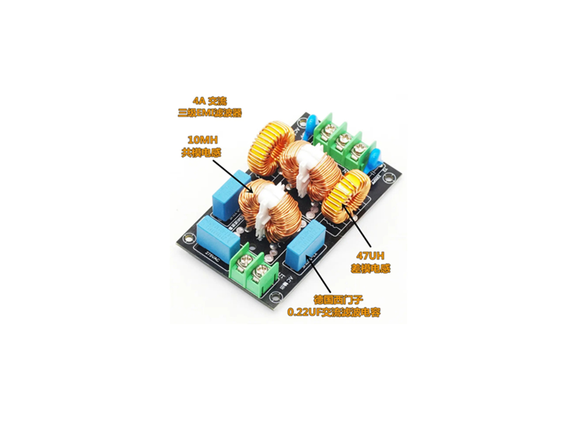
Classic AC input filter combination: Common-mode choke + X capacitor + Y capacitors
Common-mode chokes suppress common-mode noise, while controlled leakage inductance assists in filtering differential-mode interference.
X capacitors connect across line and neutral to filter differential-mode noise.
Y capacitors suppress common-mode noise; their capacitance is limited by safety regulations on total leakage current and cannot be increased arbitrarily.
Place filtering components as close to the input terminals as possible, keeping filter ground traces short and direct. Use parallel capacitors of different values to cover both low- and high-frequency ranges. Add ferrite beads to signal lines to suppress MHz-range high-frequency noise.
5. Shielding, Grounding, and Structural Support Measures
Add insulation isolation to the heatsink and ensure proper grounding. For units exceeding radiation limits, install a grounded metal shielding enclosure. Use shielded cables for long input/output lines and ground them correctly.
6. Common Design Pitfalls
❌ Relying solely on filter components while neglecting PCB layout;
❌ Blindly increasing the Y capacitor caused leakage current to exceed limits.
❌ PGND and SGND connected at multiple points, creating a ground loop.
❌ Large-area copper pouring on SW node increases radiation;
❌ Failing to plan for EMI early and waiting until prototype completion to fix issues.
7. Standard Development Process
System topology assessment → Reserve debug pads in schematics → Strictly follow EMI routing guidelines in PCB design → Locate noise sources using near-field probes on prototypes → Iteratively optimize by distinguishing common-mode vs. differential-mode noise → Conduct formal EMC lab testing.
Conclusion
Switching power supply EMI is a systemic challenge that cannot be solved by a single component. Prioritize noise reduction at the source, optimize layout and routing as the primary strategy, and use filtering circuits as supplementary measures. Integrating these considerations early in the design phase significantly reduces rework costs later and accelerates product time-to-market.